


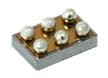
Toshiba U-MOSIII MOSFETs
Toshiba U-MOSIII MOSFETs are single- and dual-channel MOSFETs ideal for high-speed switching applications. These Toshiba MOSFETs offer a low drain to source on-resistance and a low voltage gate drive.
Features
- Logic-level gate drive
- 0.0135Ω to 6.0Ω (@VGS = -2.5V) maximum drain-source on-resistance (RDS(ON))
- -20V to +30V drain-source voltage (VDSS)
- ±8V to ±10V gate-source voltage (VGSS)
- -14A to 4.2A drain current (ID)
- 0.1W to 1.25W power dissipation (PD)
- 12pF to 3350pF input capacitance (CISS)
Applications
- Switching voltage regulators
- DC-DC converters
Application Notes
- Bipolar Transistors: Electrical Characteristics
- Bipolar Transistors: Maximum Ratings
- Bipolar Transistors: Terms
- Bipolar Transistors: Thermal Stability and Design
- Calculating the Temperature of Discrete Semiconductor Devices
- Derating of the MOSFET Safe Operating Area
- Hints and Tips for Thermal Design for Discrete Semiconductor Devices: Part 1
- Hints and Tips for Thermal Design for Discrete Semiconductor Devices: Part 2
- Hints and Tips for Thermal Design for Discrete Semiconductor Devices: Part 3
- IGBTs (Insulated Gate Bipolar Transistors)
- Impacts of the dv/dt Rate on MOSFETs
- MOSFET Avalanche Ruggedness
- MOSFET Gate Drive Circuit
- MOSFET Paralleling (Parasitic Oscillation between Parallel Power MOSFETs)
- MOSFET Self-Turn-On Phenomenon
- Parasitic Oscillation and Ringing of Power MOSFETs
- Power MOSFETs: Maximum Ratings
Related Products

Toshiba Discrete Solid State Drive (SSD) Solutions
Broad product lineup that meets the latest requirements with TVS, SBD, LDOs, and Load Switch ICs.

Toshiba TCR3UG Series Low-Dropout Regulators
Offer a fast load transient and voltage regulation up to 300mA CMOS in an ultra-small package.

Toshiba TCR3DM Series CMOS LDO Voltage Regulators
Available in fixed output voltages between 1.0V and 4.5V and capable of driving up to 300mA.

Toshiba CMOS Low Dropout Regulators
Feature low dropout (LDO) voltage, low output noise voltage and fast load transient response.

Toshiba Regulatory napięcia LDO TCR15AG
Regulatory LDO 1,5 A w obudowie WCSP6F oferują wydajne niskoszumowe zasilanie Wi-Fi, kamer i urządzeń przenośnych.

Toshiba TCKE8xx & TCKE712BNL eFuse ICs
Offers adjustable over current protection and reverse blocking FET control.

Toshiba TCK3xx Single Output Power Multiplexer ICs
Single output multiplexer load switch ICs with overvoltage protection and low switch ON resistance.

Toshiba TCK206G / TCK207G / TCK208G Load Switches
0.75V ultra-low voltage load switch ICs for power management with slew rate control driver.
Toshiba TCK10xG Load Switch ICs
Features low-voltage operation, low on-resistance, low current consumption, and a control input pin.

Toshiba U-MOSVI Small Signal MOSFETs
Supports high-current charging with low voltage and low RDS(on) requirements.
Toshiba CUHSx Schottky Barrier Diodes
Suitable for rectifying power supply circuits and protecting reverse current.

Toshiba Next-Generation ESD Protection Diodes
Used for power supply circuits in mobile devices like smartphones and wearable devices.

Toshiba U-MOSVII MOSFETs
P-channel MOSFETs featuring a low voltage gate drive and low drain-source on-resistance.

Toshiba U-MOSVII-H MOSFETs
Logic-level gate drive and low-voltage gate drive MOSFETs, offered in a wide range of SMD packages.