


Renesas Electronics RZ/T2L High-Performance MPU with EtherCAT

Renesas Electronics RZ/T2L High-Performance MPU with EtherCAT realizes high-speed processing and high-precision real-time control. RZ/T2L enables users to easily scale product development by offering a similar hardware (H/W) architecture as the RZ/T2M and a scalable/compatible software (S/W) platform with Renesas MPU and MCU. The 12mm2 x 0.8mm pitch, 196-pin FBGA packaged component operates within a -40°C to +125°C temperature range.
Features
- Integrated Arm® Cortex®-R52 at 800MHz maximum, a tightly coupled memory (576KB) directly connected to CPU and Low Latency Peripheral port (LLPP) bus
- Integrated rich peripheral functions such as ΣΔ I/F, A/D converter, and multi-protocol encoder I/F
- Seamless H/W architecture with RZ/T2M, and scalable/compatible S/W platforms, such as FSP with Renesas MPU and MCU
- Integrated EtherCAT slave controller and supports ECC for all internal RAM
- Supports security functions such as secure boot, JTAG authentication, and unique ID
- Can be used as safety MCU in the functional safety S/W solution
- High-performance real-time control
- Motor control system on a single chip
Applications
- AC servos
- Inverters
- Industrial robots
- Medical equipment
- Wind turbines
- Elevators
Specifications
- On-chip single 32-bit Arm® Cortex-R52 processor
- High-speed real-time control with an operating frequency of 200/400/800MHz
- 512KB/64KB Tightly Coupled Memory (TCM) with ECC
- Instruction cache/data cache with ECC, 16KB per cache
- High-speed interrupt
- FPU supports addition, subtraction, multiplication, division, multiply-and-accumulate, and square-root operations at single-precision and double-precision
- The NEON and Advanced SIMD support integer or single-precision results
- Harvard architecture with 8-stage pipeline
- Supports the memory protection unit (MPU)
- Arm CoreSight architecture includes support for debugging through JTAG and SWD interfaces
- Low power consumption with Standby mode and Module Stop function
- On-chip SRAM
- 1.0MB of the on-chip SRAM with ECC
- 150/200MHz
- Data transfer (DMAC: 16 channels × 2 units)
- Event link controller
- Module operations can be started by event signals rather than by interrupt handlers
- Linked operation of modules is available even while the CPU is in the standby state
- Reset and power supply voltage control, four reset sources (including a pin reset)
- Clock functions
- 25MHz external clock/oscillator input frequency
- 200/400/800MHz or 150/300/600MHz CPU clock frequency
- 200MHz or 150MHz system clock frequency
- 240kHz Low-speed on-chip oscillator (LOCO)
- Safety functions
- Register write protection, input clock oscillation stop detection, and CRC
- Master Memory Protection Unit (MPU)
- Security functions (optional)
- Boot mode with security through encryption
- JTAG authentication
- Cryptologic accelerator
- TRNG
- Encoder interfaces
- Up to 2x channels
- EnDat 2.2, BiSS-C, A-format, and HIPERFACE DSL-compliant interfaces
- Frequency-divided output from an encoder
- Communications interfaces
- Ethernet
- 3x port EtherCAT slave controller
- Single-port Ethernet MAC
- Single-channel USB 2.0 high-speed host/functions
- 2-channel CAN/CANFD (compliant with ISO11898-1)
- 6-channel SCI with 16-byte transmission and reception FIFOs
- 3-channel I2C bus interface for transfer at up to 400kbps
- 4-channel SPI
- 2-channel xSPI
- Ethernet
- External Serial Host Interface (SHOSTIF)
- External address space
- Buses for high-speed data transfer at up to 100MHz
- Support for up to 4 CS areas
- 8- or 16-bit bus space selectable per area
- Up to 35x extended-function timers
- 16-bit x 8 + 32-bit MTU3 (9 channels), 32-bit GPT (18 channels): input capture, output compare, and PWM waveform output
- 16-bit CMT (6 channels), 32-bit CMTW (2 channels)
- ΔΣ interface, Up to 6x ΔΣ modulators connectable externally
- Trigonometric function unit
- Simultaneous calculation of sine and cosine
- Simultaneous calculation of arctangent and hypot_k
- 12-bit A/D converter, 12 bits × 2 unit (4 channels for unit 0 and 1)
- Temperature sensor for measuring temperature within the chip
- General-purpose I/O ports
- Input pull-up/pull-down
- The locations of input/output functions for peripheral modules are selectable from among multiple pins
- -40°C to +125°C operating temperature range
- 12mm2 x 0.8mm pitch, 196-pin FBGA package
Block Diagram

Additional Resources
View Evaluation Kit
Related Development Tools
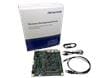
Renesas Electronics RZ-T2L Starter Kit+
Complete demonstration and development platform for the RZ/T2L High-Performance MPU with EtherCAT.
Related MPUs

Renesas Electronics RZ Family 32 & 64-bit MPUs
Offer high-performance CPU cores, various accelerators, and peripheral functions.

Renesas Electronics RZ/T2M Group Microprocessors
Highly integrated MPU optimized for motor control, industrial networking, and functional safety.