


Texas Instruments MSP430FR599x/MSP430FR596x Mixed-Signal MCUs
Texas Instruments MSP430FR599x/MSP430FR596x Mixed-Signal Microcontrollers (MCUs) take low power and performance to the next level with the unique Low-Energy Accelerator (LEA) for digital signal processing. This accelerator delivers 40x the performance of Arm® Cortex®-M0+ MCUs to help developers efficiently process data using complex functions such as FFT, FIR, and matrix multiplication. Implementation requires no DSP expertise with a free optimized DSP Library available. Additionally, with up to 256KB of unified memory with FRAM, the Texas Instruments MSP430FR599x/MSP430FR596x offer more space for advanced applications and flexibility for effortless implementation of over-the-air firmware updates. The MSP Ultra-Low-Power (ULP) FRAM microcontroller platform combines uniquely embedded FRAM and holistic ultra-low-power system architecture. This combination allows system designers to increase performance while lowering energy consumption. FRAM technology combines the low-energy fast writes, flexibility, and endurance of RAM with the nonvolatile behavior of Flash.
Features
- Embedded microcontroller
- 16-Bit RISC architecture up to 16MHz clock
- Up to 256KB of Ferroelectric Random Access Memory (FRAM)
- Ultra-low-power writes
- Fast write at 125ns per word (64KB in 4ms)
- Flexible allocation of data and application code in memory
- 1015 write cycle endurance
- Radiation resistant and non-magnetic
- 1.8V to 3.6V wide supply voltage range
- Optimized ultra-low-power modes
- Active mode (118µA/MHz)
- Standby with VLO (LPM3) (500nA)
- Standby with Real-Time Clock (RTC) (LPM3.5) (350nA)
- Shutdown (LPM4.5) (45nA)
- Low-Energy Accelerator (LEA) for signal processing (MSP430FR599x only)
- Operation independent of CPU
- 4KB of RAM shared with CPU
- Efficient 256-point complex FFT: up to 40x faster than Arm Cortex-M0+ Core
- Intelligent digital peripherals
- 32-bit hardware Multiplier (MPY)
- 6-channel internal DMA
- RTC with calendar and alarm functions
- Six 16-Bit timers with up to seven capture/compare registers each
- 32 and 16-Bit Cyclic Redundancy Check (CRC)
- High-performance analog
- 16-channel analog comparator
- 12-bit Analog-to-Digital Converter (ADC) featuring window comparator, internal reference, and sample-and-hold, up to 20 external input channels
- Multifunction input/output ports
- All pins support capacitive-touch capability with no need for external components
- Accessible bit, byte, and word-wise (in pairs)
- Edge-selectable wake from LPM on all ports
- Programmable pullup and pulldown on all ports
- Code security and encryption
- 128 or 256-Bit AES security encryption and decryption coprocessor
- Random number seed for random number generation algorithms
- IP encapsulation protects memory from external access
- Enhanced serial communication
- Up to four eUSCI_A serial communication ports
- UART with automatic baud-rate detection
- IrDA encode and decode
- Up to four eUSCI_B serial communication ports
- I2C with multiple-slave addressing
- Hardware UART or I2C Bootloader (BSL)
- Up to four eUSCI_A serial communication ports
- Flexible clock system
- Fixed-frequency DCO with ten selectable factory-trimmed frequencies
- Low-power, low-frequency internal clock source (VLO)
- 32kHz crystals (LFXT)
- High-frequency crystals (HFXT)
- Up to four eUSCI_B serial communication ports
- I2C with multiple-slave addressing
- Hardware UART or I2C Bootloader (BSL)
Applications
- Grid infrastructure
- Factory automation and control
- Building automation
- Portable health and fitness
- Wearable electronics
Block Diagram

Development Tools
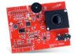
Texas Instruments BOOSTXL-AUDIO Audio BoosterPack Plug-in Module
Adds audio input functionality from a microphone and audio output through an on-board speaker.

Texas Instruments C-GANG Low-Cost Gang Programmer
Gang programmer can program up to six targets at once & is compatible with the MSPM0/MSP430 devices.
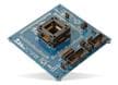
Texas Instruments MSP-TS430PN80B 80-Pin MCU Development Board
Standalone ZIF socket target board used to program and debug the MSP430 in 80-pin QFP package.
Opublikowano: 2017-03-13
| Zaktualizowano: 2025-04-16