ROHM Semiconductor SCT4062KWAHR AEC-Q101 N-Channel SiC Power MOSFET
ROHM Semiconductor SCT4062KWAHR AEC-Q101 N-Channel Silicon Carbide (SiC) Power MOSFET is a high-performance, automotive-grade device for use in demanding automotive environments. The ROHM SCT4062KWAHR features a high drain-source voltage rating of 1200V and a continuous drain current of 24A (at +25°C), making the MOSFET well-suited for high-voltage, high-efficiency power conversion systems. With a typical on-resistance of 62mΩ, the SCT4062KWAHR minimizes conduction losses and supports fast switching, which contributes to reduced power loss and improved thermal performance. Packaged in a TO-263-7LA format, the device offers excellent heat dissipation and ease of integration into compact power modules. SCT4062KWAHR is ideal for electric vehicle (EV) applications such as traction inverters, onboard chargers, and DC-DC converters, where reliability, efficiency, and thermal stability are critical.Features
- AEC-Q101 qualified
- Low on-resistance
- Fast switching speed
- Fast reverse recovery
- Easy to parallel
- Simple to drive
- TO-263-7LA package
- Wide 4.7mm (minimum) creepage distance
- Pb-free lead plating
- RoH compliant
Applications
- Automotive
- Switch mode power supplies
Specifications
- 1200V maximum drain-source voltage
- Maximum continuous drain/source current
- 24A at +25°C
- 17A at +100°C
- 80μA maximum zero gate voltage drain current
- 52A maximum pulsed drain current
- Body diode
- Maximum forward current
- 24A pulsed
- 52A surge
- 3.3V typical forward voltage
- 8.1ns typical reverse recovery time
- 105nC reverse recovery charge
- 26A typical peak reverse recovery current
- Maximum forward current
- -4V to 21V maximum DC gate-source voltage range
- -4V to 23V maximum gate-source surge voltage range
- Maximum recommended gate-source drive voltage
- 15V to 18V maximum turn-on range
- 0V turn-off
- ±100nA gate-source leakage current
- 2.8V to 4.8V gate threshold voltage range
- Static drain-source on-state resistance
- 81mΩ maximum at +25°C
- 62mΩ typical
- 4Ω typical gate input resistance
- 1.6K/W junction-to-case thermal resistance
- 6.5S typical transconductance
- Typical capacitance
- 1498pF input
- 45pF output
- 3pF reverse transfer
- 54pF effective output, energy-related
- Typical gate
- 64nC total
- 14nC source charge
- 17nC drain charge
- Typical time
- 4.4ns turn-on delay
- 11ns rise
- 22ns turn-off delay
- 10ns fall
- Typical switching losses
- 132μJ turn-on
- 6μJ turn-off
- +175°C maximum virtual junction temperature
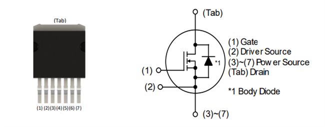
Inner Circuit

Opublikowano: 2025-06-13
| Zaktualizowano: 2025-06-19


