onsemi NxJS3151P Single P-Channel Power MOSFETs
onsemi NxJS3151P Single P-Channel Power MOSFETs are high-performance MOSFETs designed for efficient switching applications. Housed in a compact SC-88 (SOT-363) 2mm x 2mm package, these onsemi MOSFETs offer a low RDS(on) of just 45mΩ at -4.5V, enabling reduced conduction losses and improved thermal performance. With a maximum drain current of -3.3A and a drain-source voltage rating of -12V, the NxJS3151P devices are well-suited for load switching in portable and battery-powered devices. The ultra-low gate charge and fast switching characteristics contribute to enhanced energy efficiency, making the onsemi NxJS3151P Single P-Channel Power MOSFETs ideal for space-constrained designs where power density and reliability are critical.Features
- Leading Trench technology for low RDS(ON) extending battery life
- SC-88 small outline (2mm x 2mm, SC70-6 equivalent) package
- Gate diodes for ESD protection
- NV prefix for automotive and other applications requiring unique site and control change requirements; AEC-Q101 qualified and PPAP capable
- Lead-free, Halogen-free/BFR-free, and RoHS compliant
Applications
- High side load switches
- Cell phones, computing, digital cameras, MP3s, and PDAs
Specifications
- Off characteristics
- -12V minimum drain-to-source breakdown voltage
- 10mV/°C typical drain-to-source breakdown voltage temperature coefficient
- Zero gate voltage drain currents
- -1.0µA maximum at +25°C
- -2.5µA typical at +125°C
- Gate-to-source leakage currents
- ±1.5µA maximum at ±4.5VGS
- ±10mA maximum at ±12VGS
- On characteristics
- -0.40V to -1.2V gate threshold voltage range
- 3.4mV/°C typical negative threshold temperature coefficient
- 60mΩ to 160mΩ maximum drain-to-source on-resistance range
- 15S typical forward transconductance
- Charges and capacitances
- 850pF typical input capacitance
- 170pF typical output capacitance
- 110pF typical reverse transfer capacitance
- 8.6nC typical total gate charge
- 1.3nC typical gate-to-source charge
- 2.2nC typical gate-to-drain charge
- 3000Ω typical gate resistance
- Switching characteristics
- 0.86µs typical turn-on delay time
- 1.5µs typical rise time
- 3.5µs typical turn-off delay time
- 3.9µs typical fall time
- 45mΩ (at -4.5V) to 133mΩ (at -1.8V) typical RDS(on) range
- ±12V maximum gate-to-source voltage
- -2.7A to -3.3A maximum continuous drain current range
- 0.625W maximum power dissipation
- -0.7V to -0.85V typical forward diode voltage range
- -0.8A maximum body diode source current
- Maximum thermal resistance
- 200°C/W junction-to-ambient steady-state
- 141°C/W junction-to-ambient
- 102°C/W junction-to-lead steady-state
- Temperatures
- -55°C to +150°C operating junction temperature range
- +260°C maximum lead soldering temperature
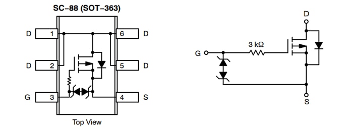
Schematic

Opublikowano: 2025-08-29
| Zaktualizowano: 2025-09-04


