


Microchip Technology MCP14T0517 Push-Pull Transformer Drivers

Microchip Technology MCP14T0517 Push-Pull Transformer Drivers are designed for compact, isolated power supplies operating from a 3VDC to 5.5VDC input. The Microchip MCP14T0517 drivers integrate two power MOSFETs and are capable of driving push‑pull, center‑tapped transformers directly from the supply. The devices feature an internal oscillator followed by a gate‑drive stage that delivers complementary outputs for ground‑referenced N‑channel power switches. Each switch includes a controlled voltage slew‑rate, and the oscillator employs frequency dithering to help reduce EMI. An external clock source may also be used when precise harmonic placement or synchronization with multiple transformer drivers is required.
Built‑in protection capabilities include a typical 2.5A peak current limit, undervoltage lockout (UVLO), thermal shutdown, and dead‑time control for the switching devices. A soft‑start function is included to limit inrush current during startup, particularly when large output capacitors are present. Two switching‑frequency options are available: MCP14T0517A operates at 150kHz for reduced EMI, and MCP14T0517B operates at 450kHz for designs requiring smaller transformers. The MCP14T0517 drivers are offered in a compact 6‑pin SOT‑23 package and are specified for operation across a -40°C to +125°C temperature range.
Features
- Integrated power switches for push-pull topology
- 3.0V to 5.5V operational input supply voltage range
- 1.7A peak drive current capability
- 150kHz or 450kHz switching frequency options
- Overcurrent and overtemperature protections
- External clock input for multiple device synchronization
- Undervoltage Lockout (UVLO) protection
- Enable function
- Internal soft-start function
- Low <1µA (typical) shutdown current
- -40°C to +125°C operating junction temperature range
- 6-lead SOT23-6 package
- AEC-Q100 automotive qualified
- RoHS-compliant
Applications
- Isolated power supplies for SiC/Si MOSFETs and IGBTs
- Bias generators for isolated communication interfaces (CAN, LIN, USB, etc.)
- Bias generators for isolated sensing circuitry
Specifications
- +6V absolute maximum supply voltage
- +15V absolute maximum D1 and D2 pins voltage
- 3.5APEAK absolute maximum switch current
- 0.5W absolute maximum power dissipation
- 3V to 5.5V operating VDD supply voltage range
- 1.5A operating output switch current
- Inputs
- 3V to 5.5V bias voltage range
- Bias currents
- 7mA maximum for MCP14T0517A, 4.5mA typical
- 9mA maximum for MCP14T0517B, 7mA typical
- 1µA maximum sleep current
- UVLO threshold
- 2.95V maximum positive-going
- 2.65V minimum negative-going
- 75mV to 125mV UVLO threshold hysteresis range
- EN, SYNC pin logic level
- 0.7V for "high"
- 0.3V for "low"
- Leakage current
- 15µA maximum on EN pin
- 1µA maximum on SYNC pin
- 1µA maximum on D1 and D2 pins
- Integrated power switches
- Switch ON-resistance at 0.5A
- 200mΩ maximum at 5V
- 350mΩ maximum at 3V
- 60V/µs typical voltage slew-rate on D1 and D2
- 50ns typical dead time
- Switch ON-resistance at 0.5A
- Oscillator
- Switching frequency ranges
- 140kHz to 160kHz for MCP14T0517A
- 420kHz to 480kHz for MCP14T0517B
- External synchronization signal on the SYNC pin
- 60kHz to 1200kHz frequency range
- 10% to 90% duty cycle range
- Switching frequency ranges
- Thermal shutdown
- +170°C typical temperature
- +20°C typical hysteresis
- +190.5°C thermal resistance per EIA/JESD51-3 standard
- ESD ratings
- ±5000V Human Body Model (HBM) per ANSI/ESDA/JEDEC JS-001, all pins
- ±2000V Charged-Device Model (CDM) per JEDEC specification JESD22-C101, all pins
Typical Application Circuit

Functional Block Diagram

Development Tools

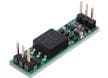
Microchip Technology EV76D05A Evaluation Board
Evaluates the performance of the MCP14T0517A and MCP14T0517B push‑pull transformer drivers.
Microchip Technology EV32R56A Reference Design
Based on the MCP14T0517B push-pull transformer driver.